-
World Leading In Surface Chemistry Instrument!
→ ADSA-RealDrop method for measuring contact angle without Axisymmetric Shape
→ Only Contact Angle meter with DSA-RealDrop method is real contact angle meter
→ Meter Using circle fitting or ellipse or tangent Is just goniometer not contact angle meter
→ World leading 3D contact angle sample stage and 3D contact angle microscope lens
→ World leading dynamic interfacial tensiometer by Wilhelmy plate method

-
Inventor of 3D Contact Angle Meter In the World!
→ Innovative development from 2D to 3D contact angle
→ New Application for contact angle hysteresis phenomenon
→ Improving the measuring accuracy of contac angle and surface free energy
→ Analysis of Heterogeneity of solid surface by 3D contact angle tool

-
We Share You More Than a Meter!
→ We are willing to share you our research and measuring experience
→ We can make special function or accessories for you to meet your application
→ More than 200 videos for solution of measuring contact angle or surface tension
→ Professional experts to give you recommend for contact angle meter or surface tensiometer
→ We have provided more than 1000 machines all over the world

-
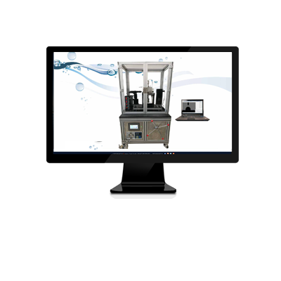
World Leading Drop Shape Analysis System C60
→ Parallel background light and telecentric lens
→ Automatic rotating stage with resolution of 0.001° for dynamic contact angle
→ 3 syringe system for automatic surface free energy measurement
→ World Leading software CAST3.0 with ADSA-RealDrop special for contact angle and surface tension
→ Modular design idea:3D contact angle, scalable extensibility, adhesive force by weight method
-
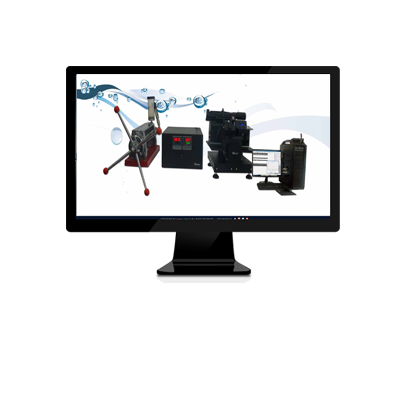
Ultra High Pressure Spinning Drop Tensiometer TX500HP
→ Max temperature 200℃, Max pressure 70MPa
→ Drop shape analysis system by spinning drop method
→ Lowest value of interfacial tension can reach 10-6mN/m under pressure conditions
→ Patent technology in China and more for your applications in the oil field
-
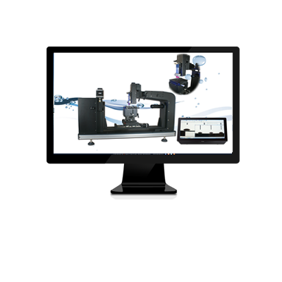
Most Popular Contact Angle Meter SL200K
→ We are the first one provide the rotating stage for standard part
→ We are the first one using multi-tilted sample stage controlled by micrometer to level the surface
→ World Leading software CAST3.0 provides ADSA-RealDrop for contact angle and surface tension
→ We are the first one using blue light LED and Color camera for measuring contact angle
→ Max 4 syringe system for measuring 8 contact angle values in one captured image
-
World Fast speed dynamic Surface Tensiometer A80
→ Adopt analytical balance with speed 92datas/second
→ Based on Young-Laplace equation correcting method by A.W.Neumann
→ Positioning Stage for sample stage using Grinding screw with 0.5mm screw pitch
→ Benefit from correcting contact angle and buoyancy, We are the only one can measure dynamic interface tension
→ Measuring density under condition of high pressure and temperature
-
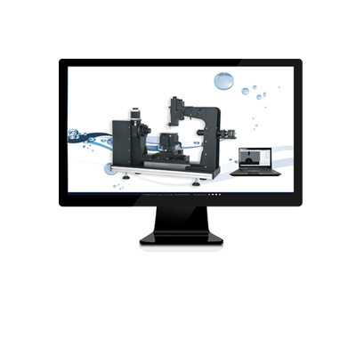
Ultra High Pressure Contact Angle Meter SL200HP
→ Provides storage tank for crude oil and piston sampling tank
→ Provides high pressure system for air such as CO2 or methane
→ Automatic constant high pressure system to provide a stabilized condition
→ Interfacial Rheometer using servo motor under high pressure and temperature condition
→ World leading software CAST3.0 using ADSA-RealDrop for contact angle, surface tension and density